What is a printed circuit board?
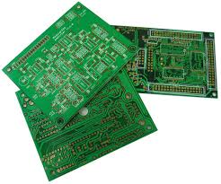
A printed circuit board (PCB) is a board made of both conducive and non-conductive materials onto which components can be soldered to create a circuit. The circuit connections are made via copper traces on the board. An example PCB is shown in Figure 1.
Figure 1: Printed circuit board |
- Dr. Jordan has created a Printed Circuit Board Overview describing the anatomy and fabrication of PCBs.
- Concepts and Terminology used in Printed Circuit Boards page from Electrosoft Engineering
Anatomy of a PCB
A PCB is made up of layers. Each layer represents a part of the manufacturing process (e.g., top and bottom copper layers, soldermask layer, silkscreen layer).
On the copper routing layers, components are soldered to copper footprints. A footprint is the physical layout on a PCB to which a component is soldered.
Each footprint has individual pads to which parts of the component (e.g., pins) are soldered.
How are PCBs manufactured?
In an industrial setting, PCBs are most commonly sent out to manufacturing houses that etch and return PCBs quickly but at very high cost. The following sites describe the PCB manufacturing process:
- Building a Printed Circuit Board from Advanced Circuits
How do we manufacture PCBs at ASU?
See the ASU PCB Fabrication Process blog entry.
