Transferring a Cadence schematic to PCB Editor
Introduction
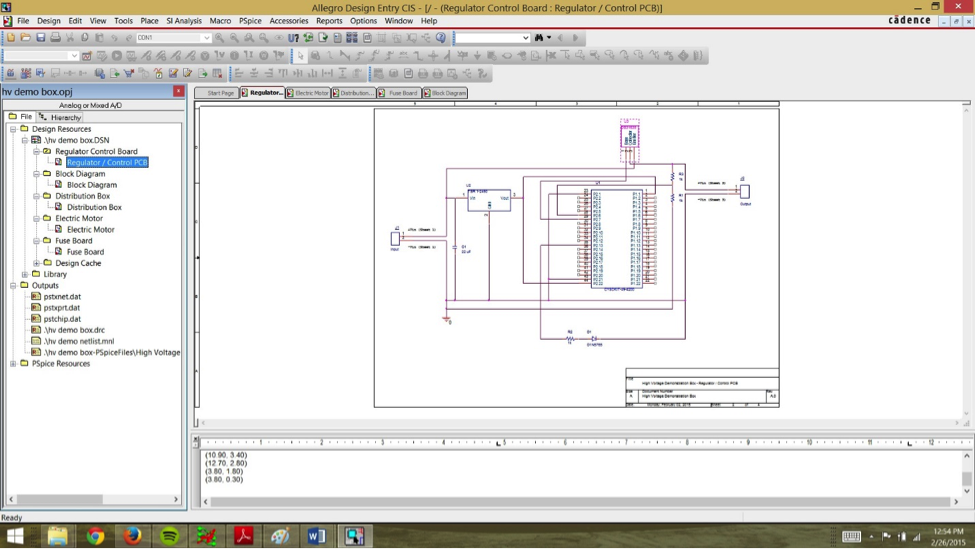
In order to create a PCB, you must first prepare the schematic and check for errors, export a netlist of the schematic, import the netlist into PCB editor, and design the PCB. A netlist is a file that describes interconnections among components in a circuit. This tutorial describes the process of transferring a schematic to PCB Editor. It is assumed that you have a completed schematic (see example, Figure 1) before trying to migrate to PCB Editor.
Figure 1: Example schematic ready for transfer to PCB Editor |
Video Walkthroughs
Cadence: Part 3 Netlist Export
Creating a PCB in Cadence PCB Editor
Create Custom Footprints
All schematic symbols need a footprint. If you created any custom schematic symbols, you likely need to create a custom footprint for each one. For most ICs, you can use the Package Designer application to make custom footprints. For all other components, you can make custom footprints manually.
Open Project and Set Root Design
-
In Windows, open your project in the Design Entry CIS program.
-
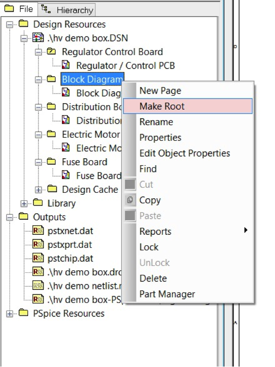
For complex designs (see example, Figure 2), you may have multiple folders with multiple schematic sheets in each folder in the project explorer. Right-click on the folder you want to prepare for transfer to PCB Editor and choose “Make Root”. This will set Cadence to generate a netlist only for the schematics inside the root folder (which will have a / through the folder symbol). This feature can be useful when your team is working on multiple break-out boards simultaneously before integrating them into one full design.
Figure 2: Example folder hierarchy for complex schematic
Assign Footprints to Components
-
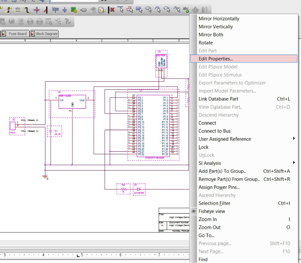
Open the schematic and select all components on the page by choosing “Edit > Select All”. Right-click and choose “Edit Properties…” (see Figure 3) to batch-edit the footprint information. The batch component property editing window will appear (see Figure 4). Click the Parts tab to show the parts in the schematic. Click the “Pivot” button to see the part information vertically instead of horizontally.
Figure 3: “Edit Properties…” menu optionFigure 4: Batch component property editing window -
Enter footprint names (built-in or custom) for each component. For more information on finding the names of built-in footprints, see Finding Existing PCB Footprints for Cadence PCB Editor. Repeat until all components have footprints.
Run Design Rules Check
-
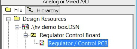
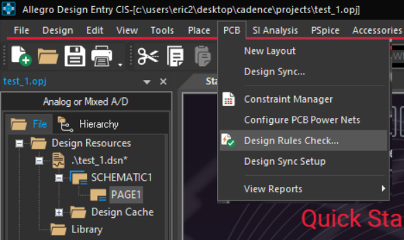
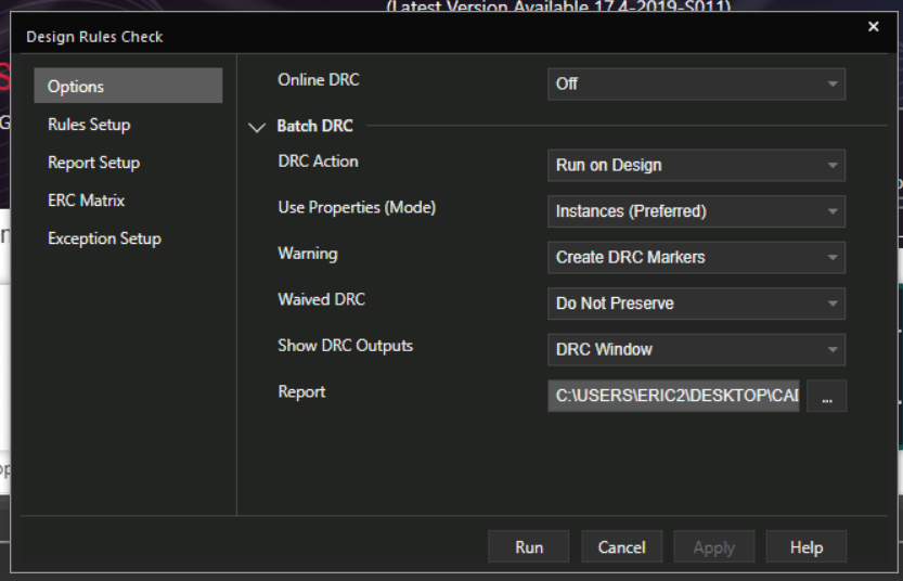
In the project explorer window, left-click on your schematic (see Figure 7) and choose “PCB menu > Design Rules Check” (see Figure 8). *(If the Design Rules Check option is dimmed, then you have selected the wrong icon in the project explorer window). *Figure 8 shows the Design Rules Check window. Leave the default options selected and click OK to continue.
Figure 7: Schematic icon selectedFigure 8: Design Rules Check… menuFigure 9: Design Rules Check window -
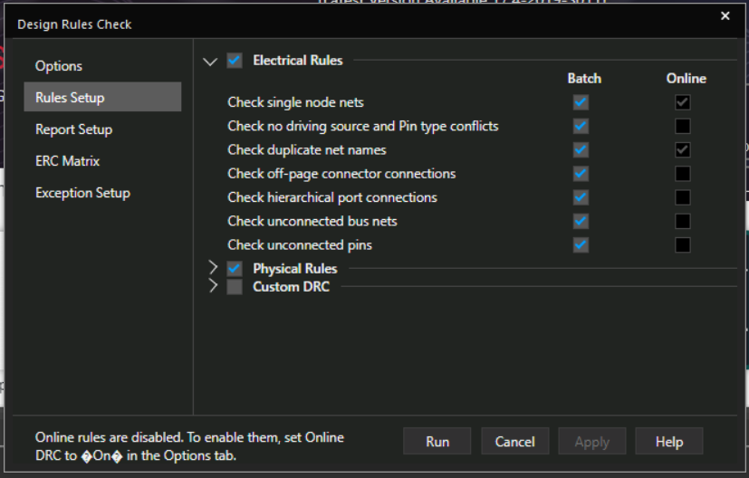
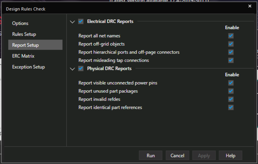
From there, you will be prompted with the DRC main screen in Figure 9. Keep everything as it is on the main screen and be sure to checkmark all of the boxes in the “Rules Setup” and “Report Setup” (see Figures 10 and 11). Doing this will ensure the DRC will check for many possible errors on the schematic. Once you have checked all of the boxes, click “Run”.
Figure 10: Design Rules Check > Rules Setup paneFigure 11: Design Rules Check > Report Setup pane -
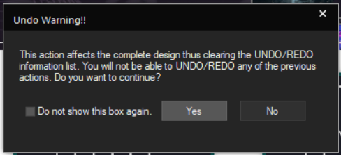
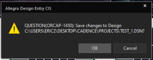
After you press “Run”, several alerts will appear. The first will be to notify you that once you proceed with the DRC, all actions already made cannot be undone (see Figure 12). Click “Yes”. The second will ask to save all the changes made since the last save (see Figure 13). Click “OK”.
Figure 12: Undo Warning alertFigure 13: Save changes alert -
In the command window, you will see a list of warnings or errors that the DRC has found. If the “DRCs” window is blank, you are ready to move on and create your PCB design. If not and an error is listed (see example, Figure 14), go back to your schematic and fix the errors. If you see warnings, read each one and consider making the recommended changes before continuing. DO NOT SKIP THIS STEP. Fix any errors identified by the Design Rules Check and repeat steps (f) - (i) until all errors are gone (or determined not to be real problems).
Figure 14: DRCs error listing
Create a Netlist
-
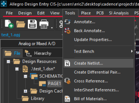
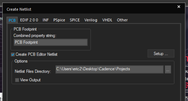
In the project explorer window, left-click on your schematic and choose “Tools > Create Netlist…” (see Figure 15). *(If the Create Netlist option is dimmed, then you have selected the wrong icon in the project explorer window). *Figure 16 shows the Create Netlist window. Set the checkboxes as shown below (file names and paths will be specific to your design) and click OK to generate a netlist as shown in Figure 16. The setlist will appear in the folder you save it to. You do not need to open the file after creating it.
Figure 15: Tools > Create Netlist… menuFigure 16: Create Netlist dialog box
Create/Update a Printed Circuit Board (PCB)
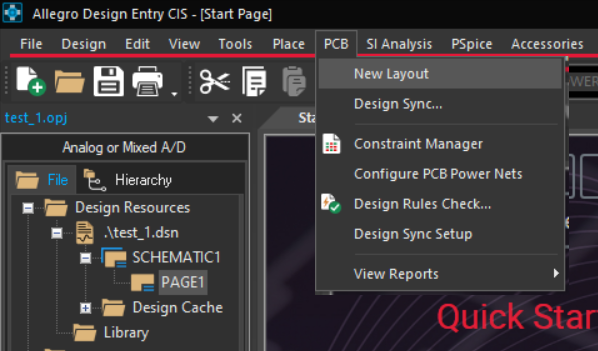
- In the Project Explorer window, left-click on your schematic and choose “PCB menu > New Layout”. (If the New Layout option is dimmed, then you have selected the wrong icon in the Project Explorer window). Figure 17 shows the New Layout window. Select the folder path where you would like yo create your new PCB design next to the “Board” path and click OK (see Figure 18). To update a PCB design you have already made, select the path where your current board is saved for “Input Board File” as well as for “Board”, and click OK (see Figure 19). Once you have clicked OK, the Allegro PCB Editor will automatically open. See the Cadence PCB Tutorials page for more information on creating a PCB.
Figure 17: PCB > New Layout menu |
Figure 18: New Layout window configured to create a new PCB design |
Figure 19: New Layout window configured to update an existing PCB design |
Common Errors
Schematic Updated after PCB is Routed
It’s not uncommon for an error to be discovered in the schematic after the PCB has already been routed. Rework of routing can be fixed as follows:
- Fix the errors in the schematic
- In the project explorer window, left-click on your schematic (see Figure 7) and choose “Tools > Create Netlist…". *(If the Create Netlist option is dimmed, then you have selected the wrong icon in the project explorer window). *Figure 9 shows the Create Netlist window. Set the checkboxes as shown above (file names and paths will be specific to your design), but this time set “Input Board File” to be your current routed PCB file and “Output Board File” to be a different name for the updated file.
- Click OK to generate a netlist and push the changes forward to PCB Editor.
Duplicate Reference Designators
Sometimes, making significant edits to a schematic can result in multiple components with the same reference designators (e.g., U1, U2, R1, R2). This can be fixed by renumbering all of the reference designators in a schematic.
- Open the project in Design Entry CIS and select the *.dsn file in the project explorer.
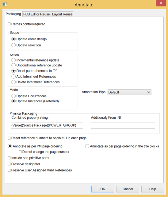
- Choose “Tools > Annotate”, select “Reset part references to”?”", and click OK (see Figure 10). Your schematic will now have ? marks for all reference designator numbers (e.g., U?, J?).
- Choose “Tools > Annotate” again, select “Incremental reference update”, and click OK (see Figure 10). This will replace all ? marks with numbers to create unique reference designators.
Figure 10: Annotate window |
Additional Common Errors
- You changed your “nets” name but missed a trace somewhere
- You changed your “nets” name and connected two different nets together accidentally (e.g., Ground_Plane and Ground)
- Cadence couldn’t find your footprint, or no footprint was specified
- Missing a *.psm file for the *.dra file, or vice-versa
- Unconnected traces
- You used multiple ground symbols and connected them together incorrectly
- Forgetting to define your paths correctly for footprints to be findable
- Defining the footprint names for all parts.
Based on a tutorial by Josh Carroll
