Printing a PCB Layout in Cadence PCB Editor
Note: This tutorial shows how to print a PCB design on paper. Please see the ASU PCB Fabrication Process for instructions on how to manufacture / “print” a PCB design in copper.
Why would you want to print a PCB design on paper?
Before sending a PCB to be manufactured, it is imperative to separate the layers and print it at 1:1 (100%) scale on paper to physically verify that your parts will fit through the holes and that pad spacing is correct.
Note: “Plot” in Cadence is synonymous with “Print” in other Windows programs
Note: You can also Print a PCB Layout in DFM Now.
How do you print a PCB design on paper?
-
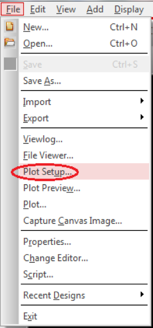
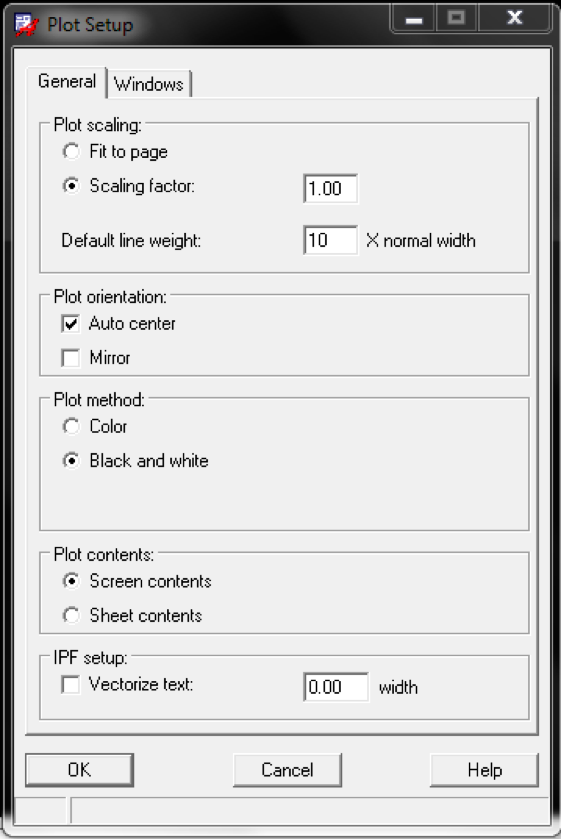
In PCB Editor, open your design and choose File > Plot Setup… (see Figure 1). The “Plot Setup” dialog box will appear (see Figure 2).
Figure 1: Plot Setup menu option -
In the “Plot Setup” dialog box, choose a “Scaling factor” of 1.00, “Auto center” checked and “Plot method” matching your printer’s capabilities (color or black and white), and click OK (see Figure 2).
Figure 2: Plot Setup dialog box -
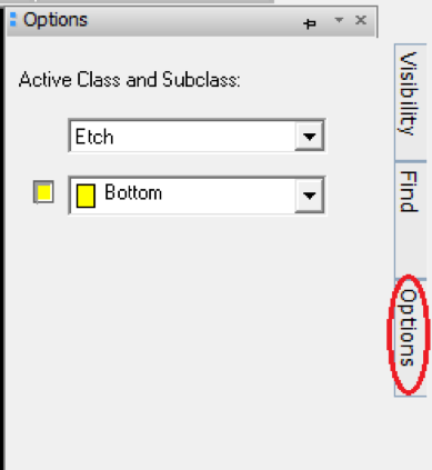
On the right side of the screen, select the Options tab. Set the “Active Class and Subclass” to Etch and the Subclass to Bottom (See Figure 3). This will show the most important details in the printout.
Figure 3: Options tab -
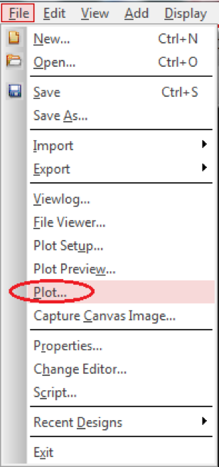
Choose File > Plot… (see Figure 4). The “Print” dialog box will appear (see Figure 5).
Figure 4: Plot menu option -
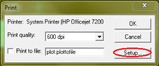
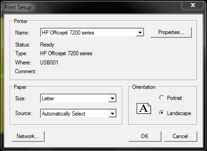
In the “Print” dialog box, click “Setup…” (see Figure 5) and select the printer, paper size, and orientation in the “Print Setup” dialog box (see Figure 6).
Figure 5: Print dialog boxFigure 6: Print Setup dialog box -
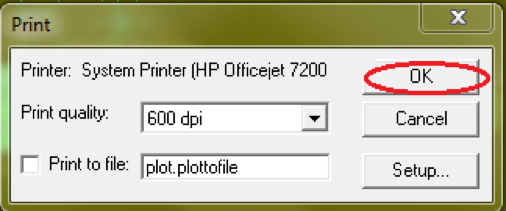
Click OK in the “Print Setup” dialog box, and OK in the Print dialog box to print the design (see Figure 7).
Figure 7: Print dialog box
Based on a tutorial by Seana O’Reilly
