Printing a PCB Design in DFM Now
Note: This tutorial shows how to print a PCB design on paper. Please see the ASU PCB Fabrication Process for instructions on how to manufacture / “print” a PCB design in copper.
Why would you want to print a PCB design on paper?
Before sending a PCB to be manufactured, it is imperative to separate the layers and print it at 1:1 (100%) scale on paper to physically verify that your parts will fit through the holes and that pad spacing is correct.
Note: You can also Print a PCB Layout in Cadence PCB Editor.
How do you print a PCB design on paper?
-
Run a Design for Manufacturing Check in DFM Now
-
In the Layer Display window, right-click on a layer and choose All Layers Off.
-
Pick a layer and click the light bulb icon next to the layer name to enable it.
-
Highlight the enabled layer in the workspace. Right-click on the enabled layer and choose Move from the contextual menu. Left-click anywhere in the workspace and then move the layer somewhere off to the side so that it won’t overlap with the other layers. Left click again. Right click anywhere in the workspace to exit the “Move” mode.
-
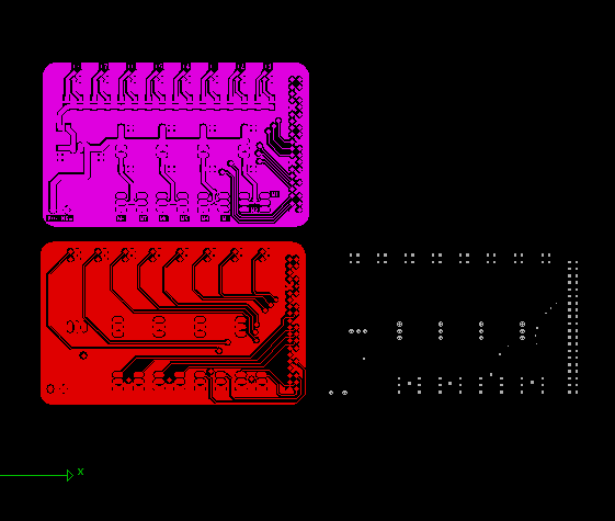
Repeat steps 3 - 5 for the remaining layers in your design (see example, Figure 1)
Figure -
Choose File > Print… and select Plot Scale : User Scale of 1.0. Click Next and PLOT! to print your design.
Based on a tutorial by Robert Goby
