Packaging Cadence Files for Submission
Introduction
This tutorial goes through how to package Cadence schematic and PCB files for submission to Canvas.
First, configure Microsoft Print to PDF to print to a file
-
In Windows, go to Settings > Devices > Printers & scanners and click on Microsoft Print to PDF. Click Manage and then Printer properties to open the “Microsoft Print to PDF Properties” window.
-
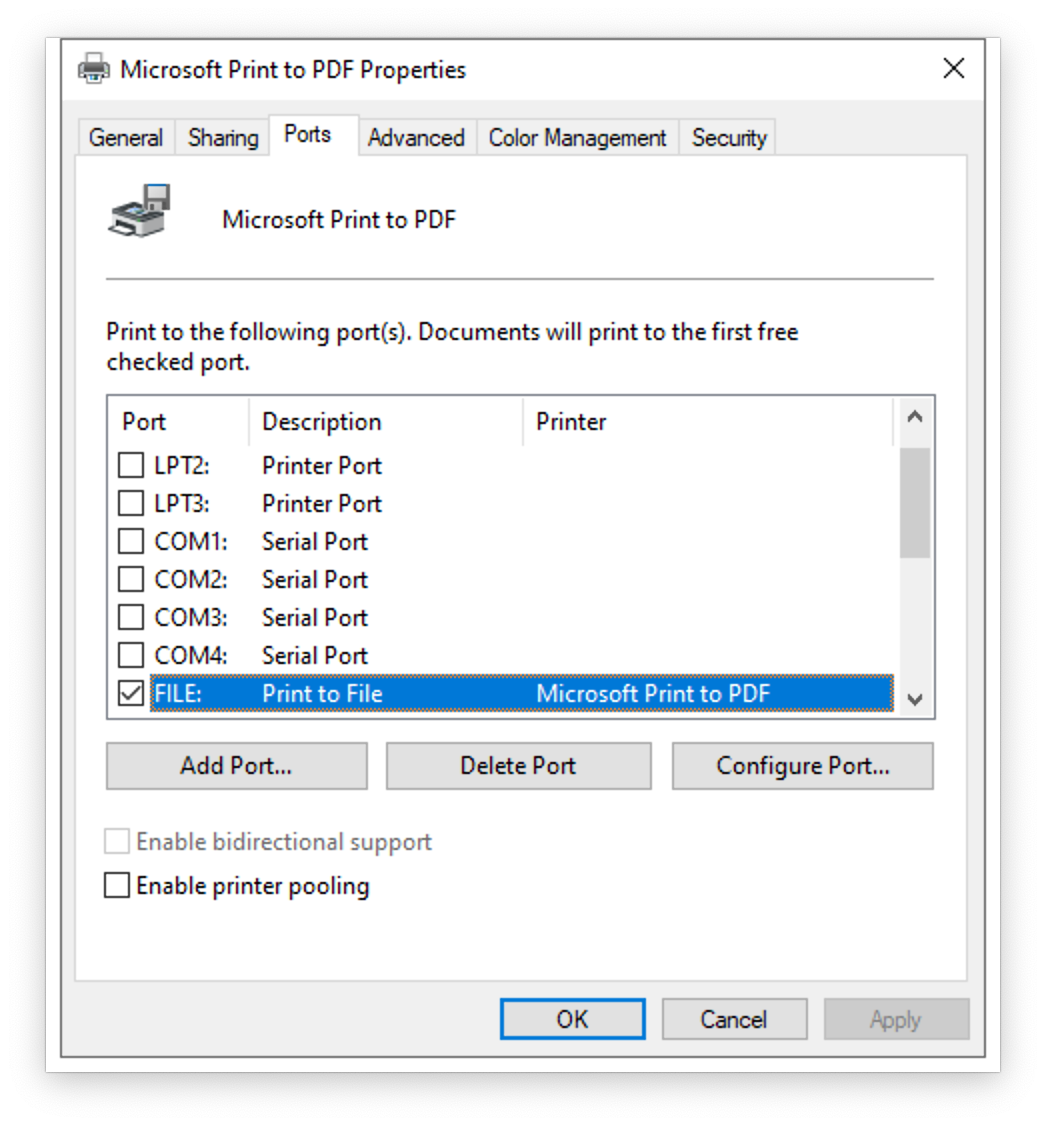
In the “Microsoft Print to PDF Properties” window, click the Change Properties button and then click on the Ports tab (see Figure 1). Select the checkbox next to FILE: Print to File and click OK.
Figure 1: Microsoft Print to PDF Properties, Ports tab
Packaging a Cadence schematic project for submission to Canvas
-
Open your schematic project in Capture CIS
First, you will convert your schematic to PDF form.
-
Choose File > Print Setup… and change the printer setup to “Microsoft Print to PDF” (or your other preferred method of printing to PDF).
-
Choose File > Print and click OK, saving your PDF to the desktop. If you are trying to expand the printout to fill a C-sized sheet, make sure to indicate that when you submit the PDF for printing to the plotter.
Next, you will ZIP the folder with your schematic project files.
-
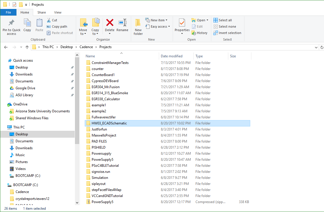
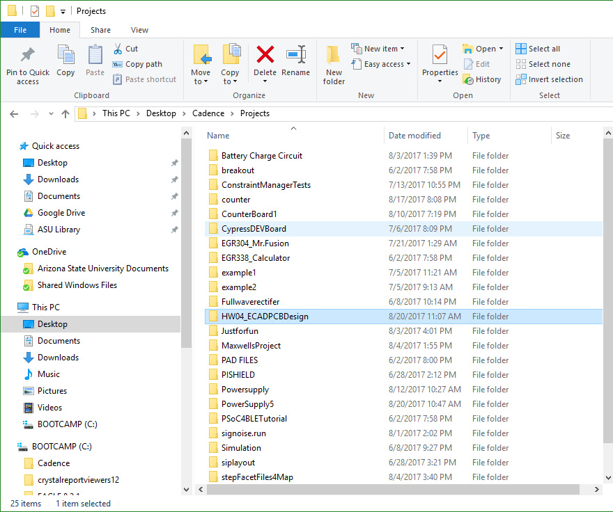
In Windows, find the project folder in which you created and saved your Cadence schematic design (see Figure 2).
Figure 2: Example of finding the schematic project folder -
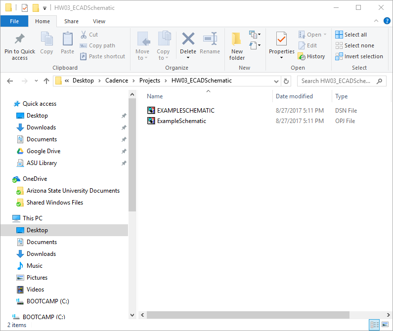
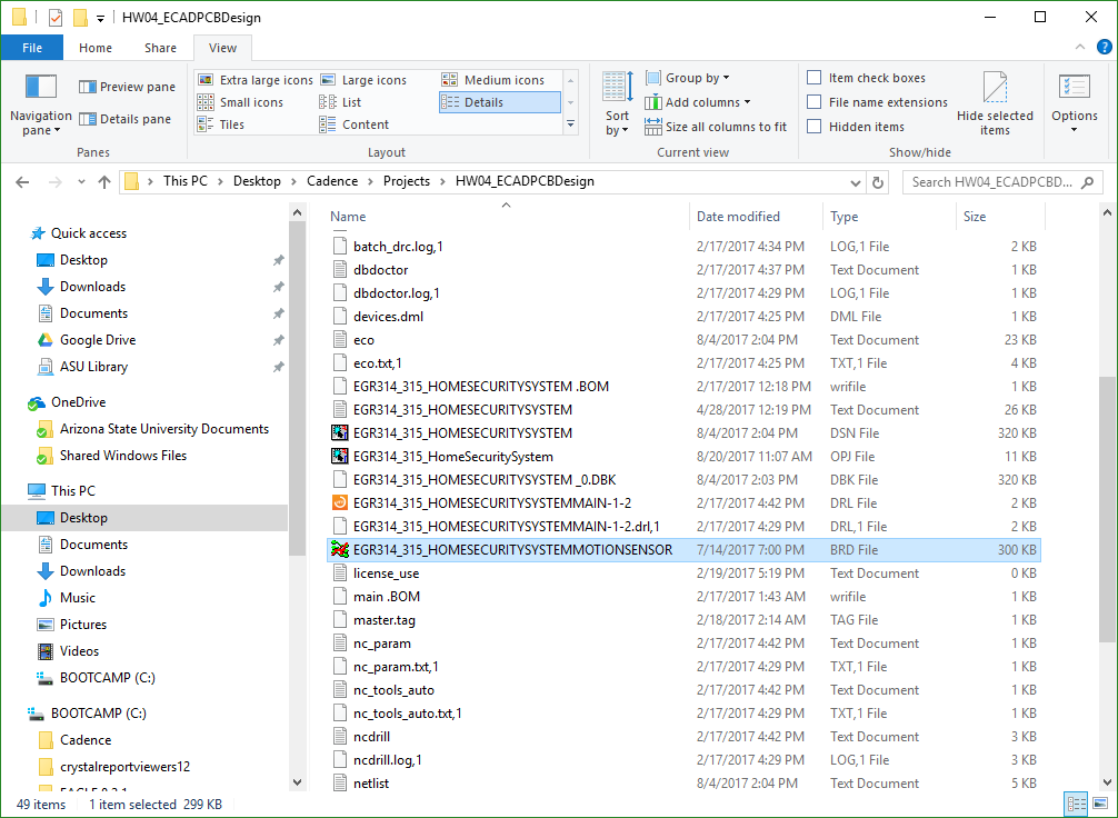
Verify that the most important files are in your project folder: (see Figure 3)
- .DSN - Cadence schematic design file
- .OPJ - Cadence schematic project file
- .OLB - Cadence schematic library file (only exists if you have a custom library)
Figure 3: Example of Cadence DSN and OPJ filesNote: You may have additional files in this folder, depending on the steps you took during the creation of your schematic. It is OK to leave additional files in the folder.
-
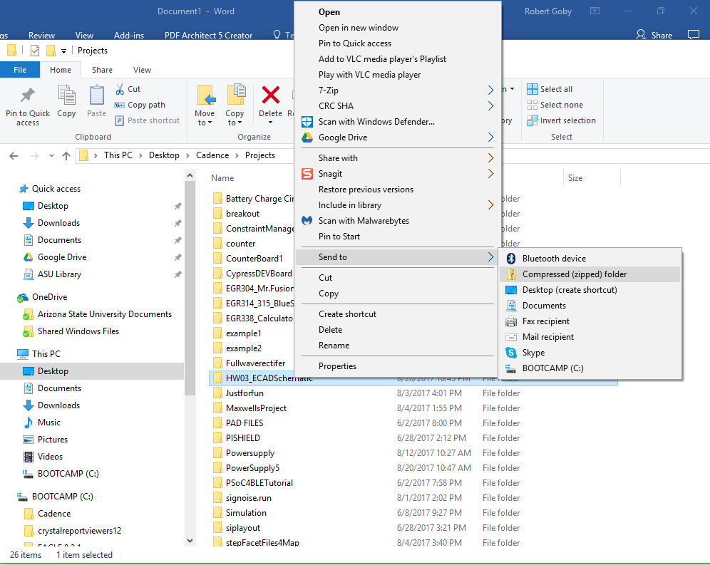
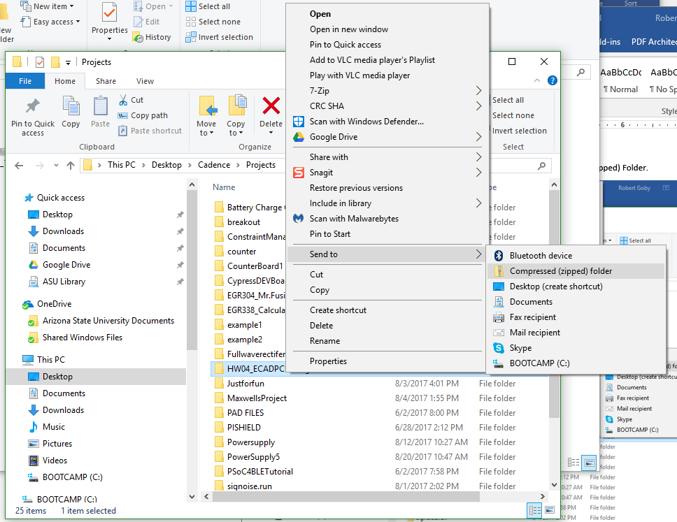
In Windows, right-click on the project folder and choose Send to > Compressed (zipped) folder (see Figure 4).
Figure 4: Creating a .zip file in Windows -
Move the .zip file to the desktop with the .pdf you created in steps 1 - 4.
-
Submit both the .pdf and the .zip file to the appropriate assignment on Canvas.
Packaging a Cadence schematic and PCB project for submission to Canvas
-
In Windows, open your PCB in PCB Editor
First, you will convert your PCB layout to .pdf form.
-
Choose File > Plot… Click “Setup…” and change the printer to “Microsoft Print to PDF”. Save the PDF file to the desktop.
Next, you will ZIP the folder with your PCB project files.
-
In Windows, find the project folder in which you created and saved your Cadence PCB design (see Figure 6).
Figure 6: Example of finding the PCB project folder -
Verify that the most important files are in your project folder: (see Figure 7)
- .DSN - Cadence schematic design file
- .OPJ - Cadence schematic project file
- .OLB - Cadence schematic library file (only exists if you have a custom library)
- .ART - Gerber files used for manufacturing
- .DRL - Drill files used for manufacturing (only exists if you have through-hole components)
- .BRD - Cadence PCB editor design file
Figure 7: Example of Cadence PCB filesNote: If you are missing any of the above files then recheck your Gerber file export process or seek additional assistance from course staff. You may have additional files in this folder, depending on the steps you took during the creation of your schematic and PCB. It is OK to leave additional files in the folder.
-
In Windows, right-click on the project folder and choose Send to > Compressed (zipped) folder (see Figure 8).
Figure 8: Creating a .zip file in Windows -
Move the .zip file to the desktop with the .pdf you created in steps 1 - 2.
-
Submit both the .pdf and the .zip file to the appropriate assignment on Canvas.
The following video shows an older version of the process described in this tutorial.
Based on a video and tutorial created by Robert Goby
