Manual Routing in Cadence PCB Editor
How do I manually route a design in PCB Editor?
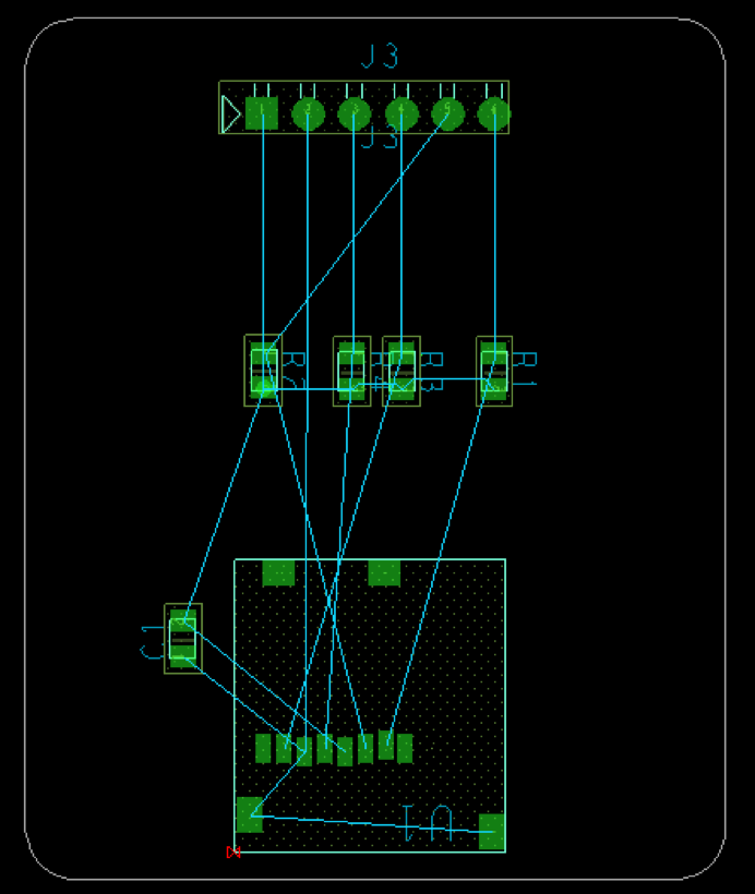
Your design should have a board outline and components placed, and blue lines (the “rats nest”) between the components (see example, Figure 1). These blue lines are not traces, but rather points that are connected on your schematic and should be converted to traces in your design.
Figure 1: Board outline, components, and rats nest |
-
Click the “Add Connect” button in the toolbar (see Figure 2)
Figure 2: Add Connect button -
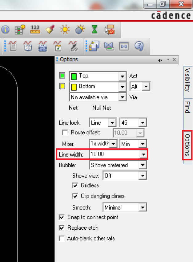
Go to the “Options” tab on the right side of the screen and change the settings for the trace as necessary (e.g., whether it will be on the top or bottom layer, which via will be used, and the line width) (see Figure 3).
*Note: *Make sure that your power and ground traces meet the recommended minimums
Figure 3: Options tab for Add Connect -
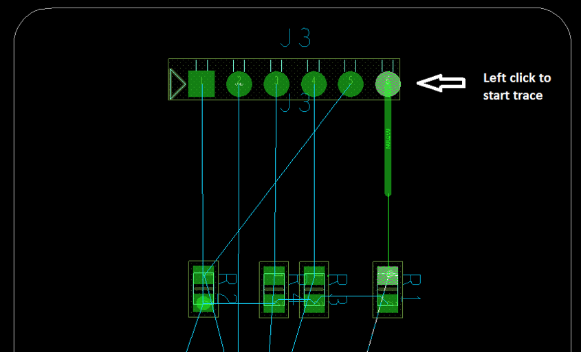
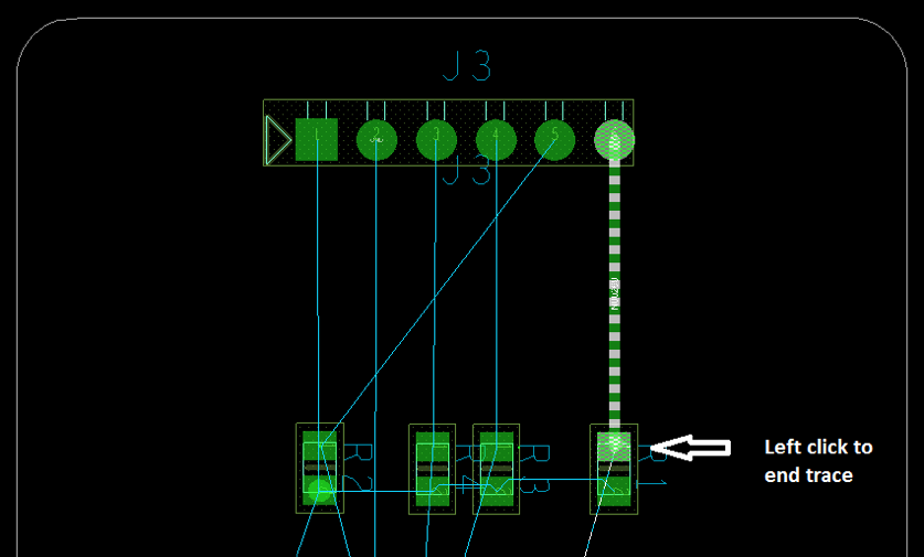
Left click on a starting pin to start the trace, and left click on the ending pin to end the trace (see Figures 4 and 5).
Note: Avoid 90 degree angles when routing traces. They create electro-magnetic radiation that interferes with other circuits.
Figure 4: Left click to start a traceFigure 5: Left click to end a trace -
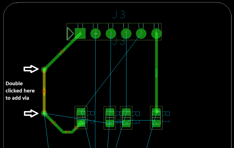
If you need to add a via (a conductive hole from one layer to another, allowing traces to cross on different layers), you can double-left click while you are placing the trace in order to change layers (see Figure 6).
Note: Vias reduce the reliability of a trace. It is recommended that you minimize the number of vias used in your design.
Figure 6: Double-left click to add a via -
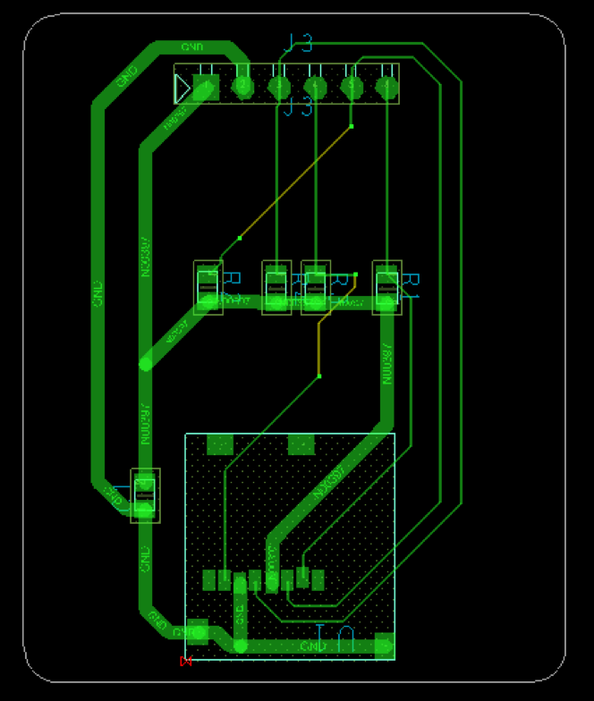
Continue the above process until all of the rats nest lines are routed (see example, Figure 7). Note that the power and ground traces are larger than the signal traces. This is important for having a fully-functioning design.
Figure 7: Example completed PCB design
Note: Manual routing of traces will almost always result in the best possible design. Auto-routing algorithms are notoriously poor and create board designs that are more complex and more difficult to debug.
Additional Resources
- How to Route Multiple Traces Simultaneously video from EMA Design Automation
Based on a tutorial by Seana O’Reilly
