Getting Started with Cadence
Introduction
A number of basic Cadence tutorial videos are available on YouTube.
Getting Started
-
In Windows, find and open the application Capture CIS (see Cadence Schematic Tutorials)
-
Create and name a new project and add existing part libraries (see Creating a New Project in Cadence)
-
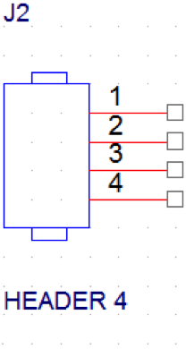
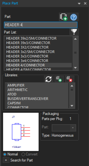
Add parts to your schematic. First, check to see if the parts you need already exist in a library. For example, schematic symbols for header pins (which are useful for connecting to components external to your custom printed circuit board, like batteries, PSoC boards, and sensors, see Figure 1) can be found by searching for “Header” in the Place Part dialog box (see Figure 2)
Figure 1: HeaderFigure 2: Place Part dialog box -
Create a custom library to store custom schematic symbols for your design that are not included in the built-in libraries (very common), and add it to your project (see Creating a Custom Library in Cadence)
-
Create and save custom schematic symbols in your custom library. If you later need to edit a custom schematic symbol, make sure to replace the edited symbol in the cache (see Creating a Custom Schematic Symbol in Cadence)
-
Create printed circuit board footprints for all components on your printed circuit board
-
For electronic devices with DIP/SOIC/PLCC/QFP/PGA/SIP/ZIP packages (which are typically integrated circuits and plug-in modules with evenly-spaced pins), it is easiest to use the “Package Symbol Wizard” (See Creating a Custom PCB Footprint using Package Designer in Cadence)
-
For all other components, create custom footprints manually (see Creating a Custom PCB Footprint Manually in Cadence)
-
Create custom padstacks for the pads of each custom footprint (See Creating a Custom Padstack in Cadence)
-
Link all footprints to schematic symbols in Design Entry CIS by updating the library search path (see Changing the Library Search Path in Cadence Design Entry CIS)
-
Link all footprints to schematic symbols in PCB Editor by updating the library search path (see Changing the Library Search Path in Cadence PCB Editor)
-
Transfer the schematic to PCB Editor for the PCB layout and design (see Transferring a Cadence Schematic to PCB Editor)
Based on a tutorial by Cody Van Cleve

