Creating a Rubout in Cadence PCB Editor
How do I create a rubout in Cadence?
-
First, make sure you have placed all of the components on your PCB (and ideally have not started routing traces yet, though this can still be done even if you have routed traces).
-
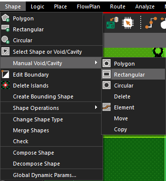
Choose Shape > Manual Void/Cavity and choose a shape of your liking (see Figure 17).
Figure 17: Anti-etch selection -
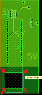
Draw an anti-etch on the appropriate layer(s) in appropriate place(s) (e.g., underneath an antenna). If there are existing races or vias in the area of the anti-etch, you will need to move them. If you have ground (or power) planes on multiple layers, you should place an anti-etch on each of the copper layers (e.g., TOP and BOTTOM). See example in Figure 18.
Figure 18: Anti-etch example under a PSoC 5 footprint -
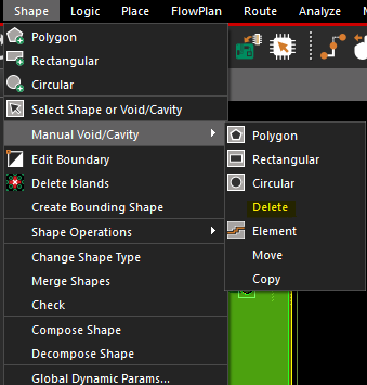
To delete an anti-etch, you need to use the special delete tool in the Manual Void/Cavity menu (see Figure 19).
Figure 19: Delete tool for manual void/cavity -
When generating your final Gerber files, you will need to add these anti-etches to the layers in the Artwork Control Form in order for them to be manufactured (see How do I export Gerber files from Cadence?).
Additional Resources
- Tutorial on Split Planes from parsysEDA
* Based on a tutorial by Cody Van Cleve and updated by Jacob Lara


