Creating a custom schematic symbol in Cadence
Introduction
In most designs, some components will not be available in built-in libraries. The purpose of this tutorial is to show how to make a custom schematic symbol that can be used in the design of schematics in Cadence.
The example custom schematic symbol created in this tutorial will be a Texas Instruments CC2541 Bluetooth-enabled microcontroller.
Limitations
This guide will not cover how to add the custom fields required for PSpice simulations. Unless you are planning to run circuit simulations, PSpice models are not required (and are often not part of the built-in parts).
1. Search the Datasheet for the Pin Layout
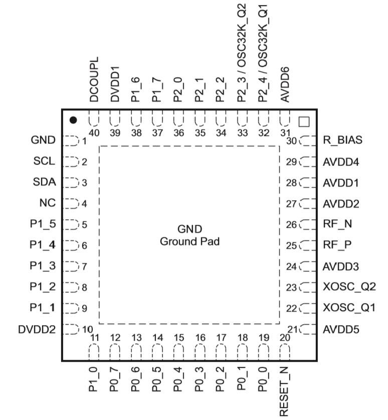
In order to build a custom schematic symbol, you need to find the pin layout in the data sheet of the component. Figure 1 shows the pin layout from the CC2541 datasheet.
Figure 1: Pin layout for the CC2541 microcontroller |
2. Create a New Project and Custom Library
See the Creating a New Project in Cadence page for instructions.
3. Create a New Schematic Symbol
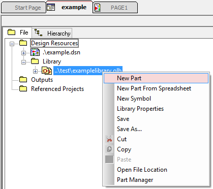
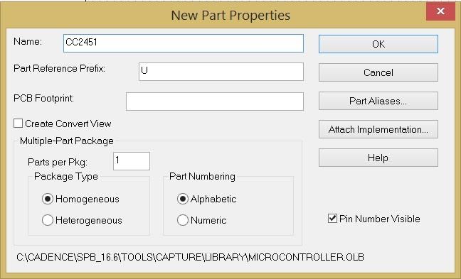
Right-click on your custom library and choose “New Part” (see Figure 2). The New Part Properties window will appear (see Figure 3). Note that the file path at the bottom of the window will be the path of your custom library.
Figure 2: Creating a new part in your custom library |
Figure 3: New Part Properties window. |
Name your part with the part number from the component datasheet. If you have not yet created a footprint for your part, you can add it at a later time.
Next, use the Place Rectangle tool in the toolbar (see Figure 4) to make an outline for your part within the dashed lines. If the area enclosed by the dashed lines is not big enough, you can enlarge it with the arrow tool. IEEE schematic formatting standards dictate that schematic symbols are usually rectangular.
Figure 4: Place rectangle tool |
Once your rectangle is complete, you can begin placing pins using the Place Pin tool in the toolbar (see Figure 5). It is a good idea to place pins on the same sides of the chip as its physical layout (see the data sheet) to make circuit debugging easier. In the case of the CC2541, there are 10 pins on each side for a total of 40 pins.
Figure 5: Place pin tool |
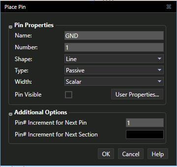
Upon clicking the Place Pin tool, a window will appear (see Figure 6). The name should be the same as the pin name in the data sheet but different than all other pins on the chip. If there are multiple pins with the same name in the data sheet, add a number to each one to differentiate (e.g., GND1, GND2). The pin number should be the pin number on the chip package, which can also be found in the data sheet. The shape can be a line (common) or other shape depending on the function of the pin. The pin type can be passive, but setting the pin type correctly will help the Electrical Rules Check (ERC) find errors in your design more easily. When you are finished configuring the pin, click OK.
Figure 6: Place Pin window |
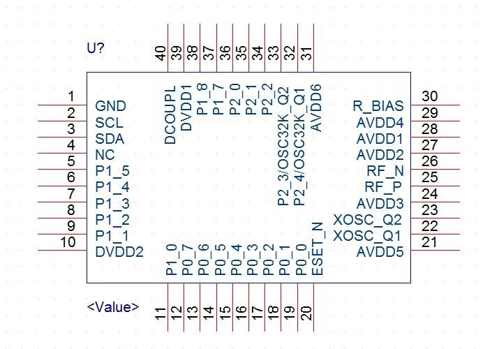
Once you are finished adding all of the pins for the component, your final product should look something like the symbol in Figure 7.
PRO TIP: When designing a custom schematic symbol, consider the schematic in which it needs to fit. The location of the schematic pins in the custom schematic symbol need not be identical to the physical part, but changing the order might complicate troubleshooting for beginners.
Figure 7: Completed schematic symbol |
Finally, save your part by choosing “File > Save As…” and double-checking to make sure it is saving to your custom library. Do not use spaces in filenames. Your custom schematic symbol will now be stored in your custom library and will be available for placing into your schematic.
4. Editing a Custom Schematic Symbol
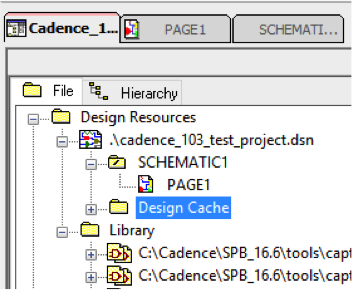
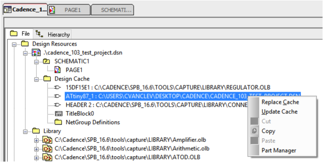
If you need to edit a custom schematic symbol, save the symbol first. Then, open the Design Cache folder in the project browser (see Figure 8), right-click on the edited schematic symbol in the design cache, and select “Replace Cache” from the drop down menu to update the schematic symbol in your schematic (see Figure 9)
Figure 8: Design Cache folder |
Figure 9: Right-click menu options |
Based on tutorials by Josh Carroll, Cody Van Cleve, and Robert Goby
