Creating a custom PCB footprint manually in Cadence
Introduction
A PCB footprint is the physical layout on a PCB to which a component is soldered. Usually, you must create a custom PCB footprint for each custom schematic symbol that you create. Footprints can be made for many standard components (e.g., basic ICs) using the Package Symbol Wizard (see the Creating a PCB footprint using Package Designer in Cadence page), but more complex components (like switching power supply ICs with thermal reliefs) must be created by hand. This tutorial details the manual creation of a custom footprint.
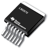
The example custom PCB footprint created in this tutorial will be a TI LM2676 SIMPLE SWITCHER 8V to 40V, 3A Low Component Count Step-Down Regulator (see Figure 1).
Figure 1: LM2676 Switching Power Supply IC |
Search the Datasheet for the Footprint Specifications
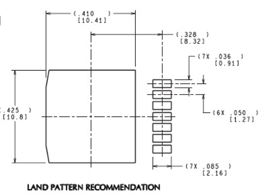
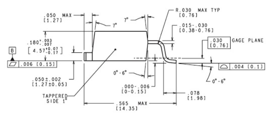
In order to build a custom footprint, you first need to find the footprint (sometimes called “land pattern” specifications in the datasheet for the component. Figures 2 and 3 show the land pattern and physical dimensions of the IC package from page 34 of the LM2676 datasheet.
Figure 2: Land pattern from the LM2676 datasheet. Dimensions are in mils, with brackets in mm. |
Figure 3: Physical package dimensions from the LM2676 datasheet. Dimensions are in mils, with brackets in mm. |
By interpreting Figures 2 and 3, the following key dimensions were determined:
Package geometry (overall)
- Length = 565 mils
- Width = 410 mils
Mechanical/Thermal Un-Plated Pad (underneath the body of the chip)
- Length = 410 mils
- Width = 425 mils
Pad - Pins
- 7 total pins
- Pad length = 36 mils
- Pad width = 85 mils
- Pad spacing = 50 mils (center of one pad to center of the next pad)
Create Custom Padstack(s)
For each different type of pin/pad, you need to create a custom padstack. For more information, see the Creating a custom padstack in Cadence page. For this example, you will need to create two custom padstacks using the dimensions above: one for the mechanical pad and one for the pin pads (which are all the same, so one padstack can be used).
Create a New Footprint
-
In Windows, open the PCB Editor application. (You can also use the Package Designer application).
-
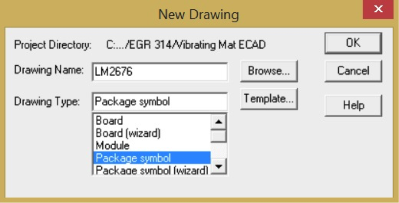
Choose “File > New…”. The New Drawing window shown in Figure 4 will appear.
Figure 4: New Drawing window -
Name your drawing, select “Package symbol” and click OK. A blank package workspace will appear.
-
Since the component footprint is a rectangle (common), choose the “Shape Add Rect” tool (see Figure 5).
Figure 5: Toolbar -
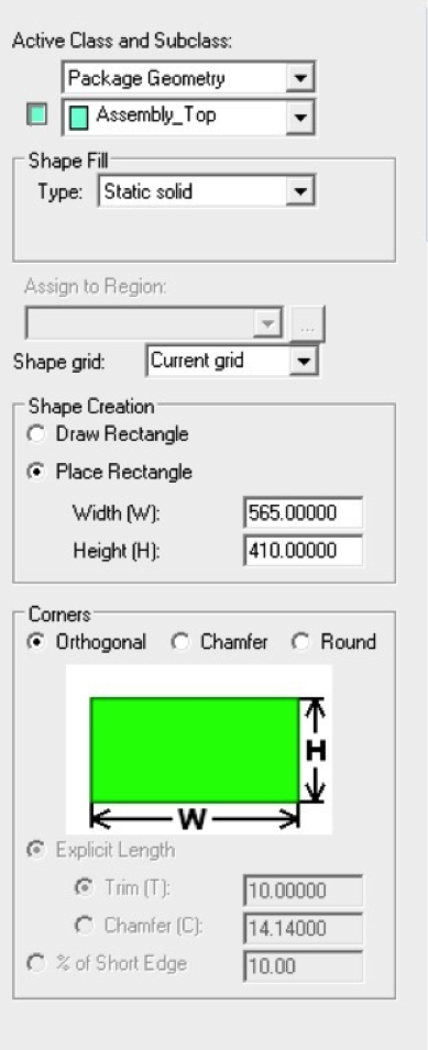
Move the cursor over the “Options” tab (see Figure 6) and enter the package geometry information from the datasheet. Then, place the rectangle on the blank workspace.
Figure 6: Options tab -
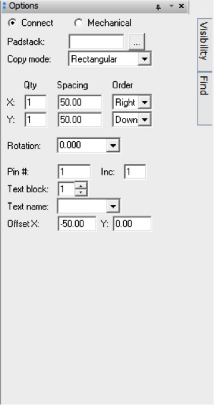
Choose “Layout > Pins” to switch to pin mode. Move the cursor over the “Options” tab (see Figure 7). The options available in the tab are described below.
Figure 7: Layout > Pins - Options tabThe Connect and Mechanical options allow a choice between an electrical pin (Connect) and a mechanical or thermal relief (described in step i below).
The Padstack box and the “…” button allow entry of the path to the padstack file. These can be the same or different for each pin, depending on the land pattern in the component datasheet.
The Copy mode option allows selection of the coordinate system for your pins. Rectangular (default) is most common.
The X and Y options allow entry of the quantity, spacing (in mils), and order of pins being placed at once. Note that multiple pins placed this way will all use the same padstack (which in most cases is fine).
The Rotation option dictates which way the padstack will be rotated. This is particularly relevant when pins are wrapped around multiple sides of an IC (e.g., for a microcontroller).
The Pin # and Inc options allow entry of the starting pin number for the first pin and the number by which to increment pin numbers when multiple pins are placed simultaneously. Make sure that these pin numbers align with the pin numbers in the custom schematic symbol that you created.
The Text block and Text name options allow association of a name with the part.
The Offset X and Y options allow correction of spacing errors. If you have created your footprint correctly up to this point, you should not need this option.
-
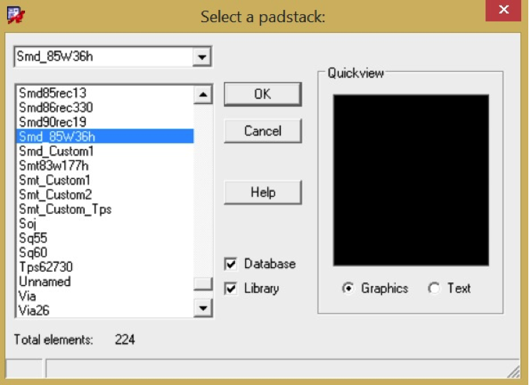
Click on the “…” button next to Padstack. The “Select a padstack:” window will appear (see Figure 8). Make sure that both “Database” and “Library” are checked, and select the custom padstack that you created for the electrical pad. In this example, the custom padstack is called “Smd_85W36h”, meaning that it is a surface mount part that is 85 mil wide and 36 mil high. Click OK.
Figure 8: Select a padstack window for electrical pad -
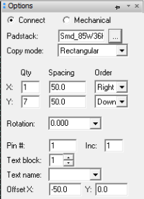
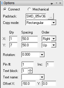
Configure the rest of the Options window as shown in Figure 9 and click to place the first pin in the correct position inside the rectangle. The result (top view) should look like Figure 10.
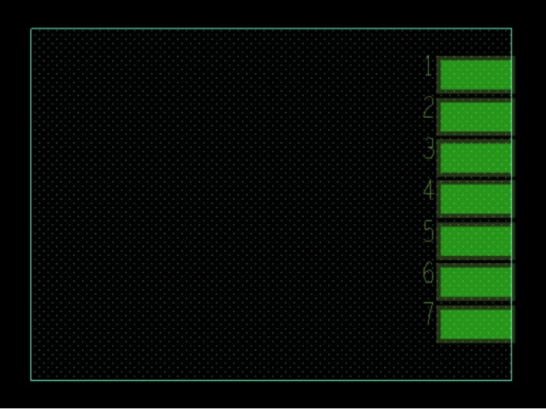
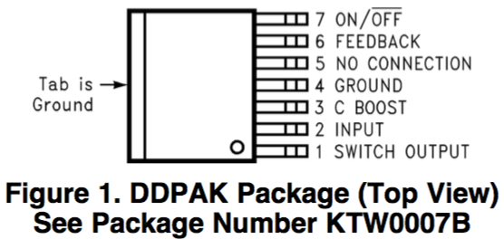
Figure 9: Options for adding 7 custom padsFigure 10: Pins added to footprintThis is a good time to double-check the data sheet connection diagrams to make sure the pin numbering is correct. Figure 11 shows the connection diagram for the IC package from page 2 of the LM2676 datasheet.
Figure 11: Connection diagram from LM2676 datasheetCareful examination shows that our new symbol has pin 1 at the top of the footprint, whereas the datasheet indicates that pin 1 should be at the bottom of the footprint. This is a critical detail (and common mistake) that must be fixed in order for the board to work properly.
There are two ways to fix this problem.
OPTION 1: Delete and replace. Right-click in the workspace and choose “Done”. Then, right-click on each pin and choose “Delete”. Finally, re-place the pins using the corrected options shown in Figure 12.
Figure 12: Corrected options for adding 7 padsOPTION 2: Manually Edit Text. Click the “Text Edit” tool in the toolbar (the bottom icon in Figure 13). Edit the number on each pin to correct it.
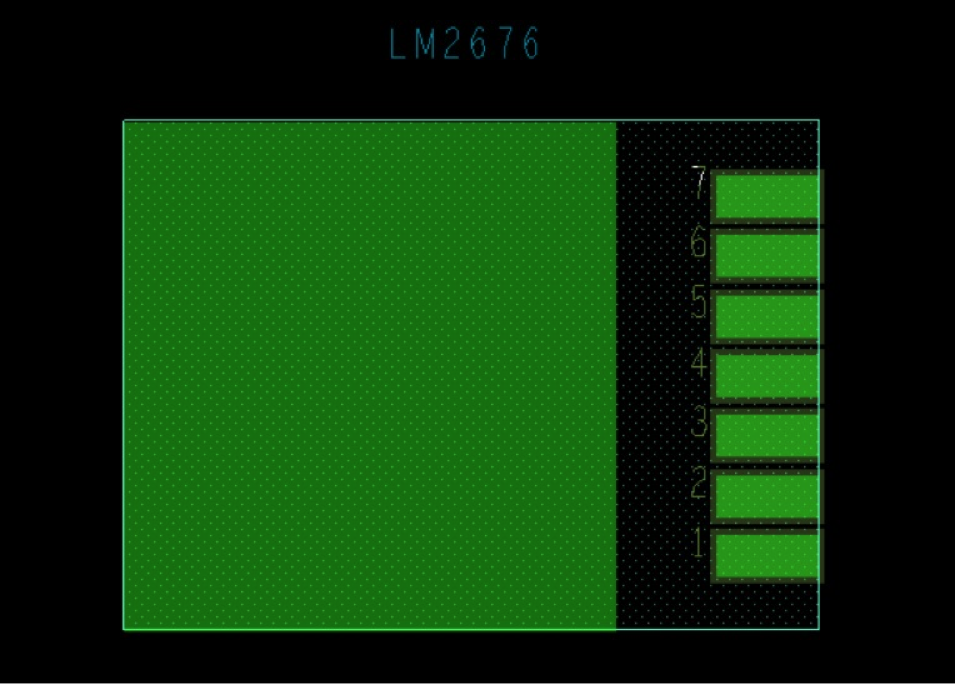
Figure 13: Toolbar with Text Edit tool (bottom)The corrected footprint is shown in Figure 16.
-
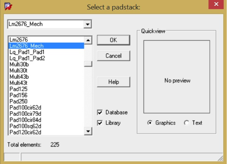
Next, add the mechanical pad. Choose “Layout > Pins” to switch to pin mode. Move the cursor over the “Options” tab and click on the “…” button next to Padstack. Select the custom padstack that you created for the mechanical pad. In this example, the custom padstack is called “Lm2676_Mech” (see Figure 14). Click OK and place the pad in the correct position inside of the rectangle.
Figure 14: Select a padstack window for mechanical pad -
Finally, you need to add a reference designator (RefDes) for the part number (in this example, LM2676) to the diagram. Click the Label Refdes tool (R1 button, second from the right in Figure 15) and add the part number above the footprint.
Figure 15: Label Refdes tool (second from right) -
Finally, choose “File > Save As…” and save the footprint to your project folder. Do not use spaces in file names. Note that the Package Wizard creates two files: a DRA file (drawing of the package) and a PSM file (package symbol, footprint). The finished PCB footprint is shown in Figure 16.
Figure 16: Finished PCB footprint
Additional Resources
- Making and Editing Footprints - Chapter 8 in the Complete PCB Design Using OrCAD Capture and PCB Editor book by Kraig Mitzner
- How to Create Complex Footprints video from parsysEDA
- OrCAD Tutorials
Based on a tutorial by Josh Carroll
