Creating a Custom Padstack (old)
Introduction
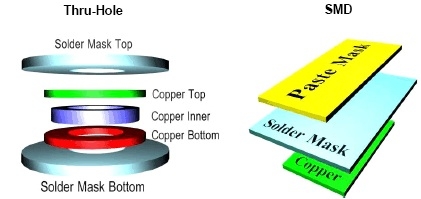
A padstack is a design for the exposed copper surface area for each hole or pad on the board where the component is mounted and soldered (see example, Figure 1). You may need to create a custom padstack when creating custom parts to ensure that the pad and hole are big enough to be reliable. This tutorial describes the manual creation of custom padstacks using the Pad Designer application.
|
|---|
Figure 1: Padstack examples for through-hole and surface mount devies |
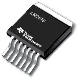
The example custom padstacks created in this tutorial will be for TI LM2676 SIMPLE SWITCHER 8V to 40V, 3A Low Component Count Step-Down Regulator (see Figure 2).
|
|---|
Figure 2: LM2676 Switching Power Supply IC |
Search the Datasheet for the Footprint Specifications
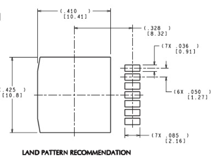
In order to build a custom padstack, you first need to find the footprint (sometimes called “land pattern” specifications in the datasheet for the component. Figure 2 shows the land pattern of the IC package from page 34 of the LM2676 datasheet.
|
|---|
Figure 3: Land pattern from the LM2676 datasheet. Dimensions are in mils, with brackets in mm. |
By interpreting Figure 3, the following key dimensions were determined:
Pad - Pins
- 7 total pins
- Pad length = 36 mils
- Pad width = 85 mils
- Pad spacing = 50 mils (center of one pad to center of the next pad)
Mechanical/Thermal Un-Plated Pad* (underneath the body of the chip)*
- Length = 410 mils
- Width = 425 mils
Create a Custom Electrical Padstack
7 pins of the LM2676 will be soldered to (7) 36 mil x 85 mil (L x W) pads spaced 50 mils apart (center to center). Since the 7 pads are all the same, we can create a single padstack and use it for all of the pins.
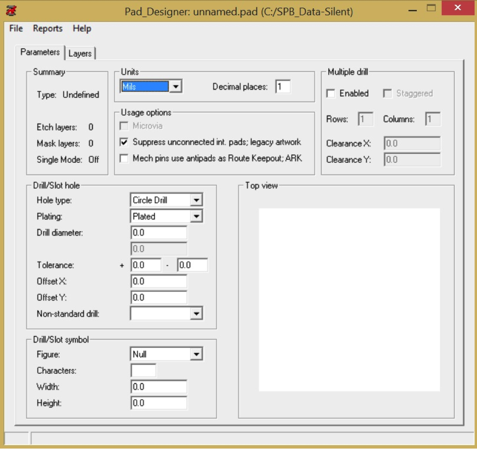
- In Windows, open the “Pad Designer” application. The Pad Designer window shown in Figure 4 will appear and default to editing the parameters for a new unnamed padstack. For a surface mount padstack, the options on the Parameters tab can be left at their defaults.
|
|---|
Figure 4: Pad Designer window, Parameters tab |
The Summary box shows the overall specifications for the currently loaded pad.
The Units box shows the units to be used in the creation of the pad, and the number of decimal places that can be used to specify a unit. The mil (1/100th of an inch) is standard for most electronic applications. Higher precision numbers may not improve the overall accuracy due to limitations in manufacturing processes.
The Usage options box shows several unused options for padstacks.
- Microvias (option usually dimmed) are tiny laser-drilled holes used to improve the electrical connection between the layers of a multilayer PCB.
- “Suppress unconnected int. pads; legacy artwork” allows for the use of older pads in new designs. Since we are only able to print double-layer (two-sided) PCBs, this option can remain unselected.
- “Mech pins use antipads as Route Keepout; ARK” limits routing of traces near mechanical (e.g., thermal or mechanical attachment) pads on the PCB. This option can remain unselected.
The Multiple drill box is not used.
The *Drill/Slot hole *box shows multiple options for padstack holes. 3 hole types are supported:
- **Circle Drill - most common **(even if the part is surface mount and has no holes)
- Oval Slot - uncommon.
- Rectangle slot - used when cutting slots around pads. Uncommon.
Plating is a conductive coating that makes a connection through holes in a PCB. 3 plating types are supported:
- **Plated - most common. **A pad will be created and then a hole will be drilled through the pad. Then, the hole will be plated after the PCB mill is finished.
- Non-plated - uncommon. An area without copper will be milled, and then a hole will be drilled through the PCB. The Thieving tool is more effective for creating mounting holes.
- Optional - uncommon. This allows the computer to decide.
Drill diameter - this is where you will enter the diameter (in the units specified above) of the drill hole. Applies to through-hole designs only.
Tolerance - uncommon (leave 0.0). Acceptable tolerances for drilling that are communicated to the PCB mill. A tolerance of 0.0 means that the hole should be as close to the actual dimensions as possible.
Offset X and Y - uncommon (leave 0.0). This allows for corrections if the PCB mill is drilling holes in the wrong places. This can be fixed more easily in the PCB mill control software.
Non-standard drill - uncommon (leave blank). This option allows for methods of drilling that are beyond what we have available.
The Drill/Slot symbol box allows for the creation of silkscreen shapes around the pad. Circle and square are most typical.
The Top view box shows the padstack under design.
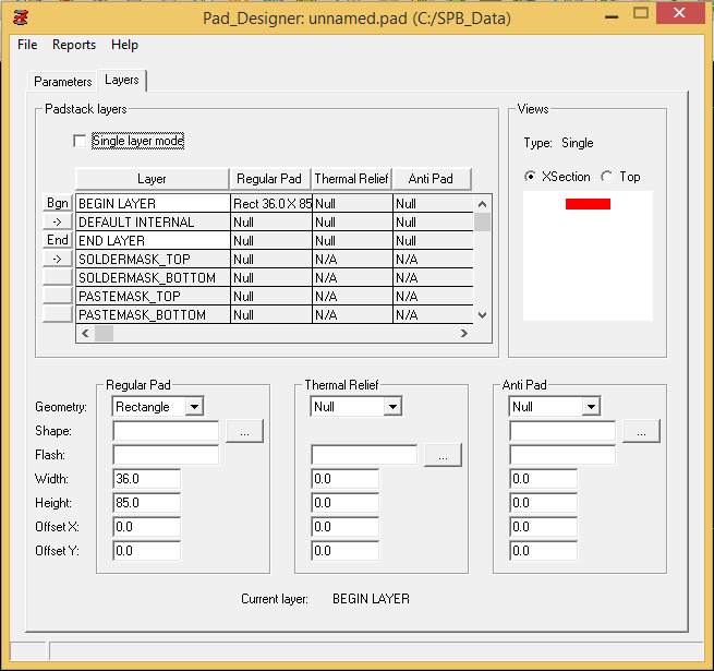
|
|---|
Figure 5: Pad Designer window, Layers tab |
The Layers tab is shown in Figure 5.
The *Padstack layers *box provides options for editing individual layers or the entire PCB. The “Single layer mode” allows for simplifying the padstack for a single-sided (single-layer) board. You can click on layers and make changes via the Regular Pad, Thermal Relief, and Anti Pad boxes described below.
The default layers for a padstack are:
- BEGIN LAYER - top copper layer of the PCB
- DEFAULT INTERNAL - inner layers of the PCB (our PCB mill is limited to 2 layers)
- END LAYER - bottom copper layer of the PCB
- SOLDERMASK_TOP - top colored soldermask layer of the PCB
- SOLDERMASK_BOTTOM - bottom colored soldermask layer of the PCB
- PASTEMASK_TOP - top solder paste layer of the PCB (uncommon in class)
- PASTEMASK_BOTTOM - bottom solder paste layer of the PCB (uncommon in class)
- FILMMASK_TOP - top conformal coating layer of the PCB (uncommon in class)
- FILMMASK_BOTTOM - bottom conformal coating layer of the PCB (uncommon in class)
The Views box shows the current padstack under design, either as a horizontal cross-section or a top view. The Regular Pad box allows editing of the size of the pad itself. The Thermal Relief box allows editing for the thermal relief pads necessary for parts that create a lot of heat (e.g., high-power MOSFETs and voltage regulators). The Anti Pad box allows editing of the keep-out area that limits the space that can be milled around the pad. All three types have the following options:
- Geometry - shape of the pad (circle, square, and rectangle most common). Set “Thermal Relief” and “Anti Pad” to Null if you do not want to use them.
- Shape - allows the creation of custom pad shapes. Especially useful for complex SMD devices.
- Flash - uncommon. Allows the protection of a layer from heat stress.
- Width and Height- size of the pad on the PCB
- Offset X and Y - uncommon. This allows for corrections if the PCB mill is not aligned. This can be fixed more easily in the PCB mill control software.
In this example, the pad dimensions from the datasheet are entered to create the pad shown in Figure 4.
Finally, choose “File > Save As…” and save the padstack to your project folder with a useful name (e.g., “SMD85W36L” which means a surface mount pad with width of 85 mil and length of 36 mil). Do not use spaces in filenames.
Create a Custom Mechanical Padstack
In this example, there is also a mechanical pad with dimensions 410 mils x 425 mils (L x W). Follow the instructions above to create the mechanical pad as a “Thermal Relief” instead of a “Regular Pad”.
“File > Save As…” and save the padstack to your project folder with a useful name (e.g., “LM2676mech”). Do not use spaces in filenames.
Additional Resources
- Part 19: Designing Pads video from iEngineered
Based on a tutorial by Josh Carroll