Changing the Library Search Path in Cadence Design Entry CIS
Why would I need to change the library search path?
When creating a custom PCB footprint for a component, it is stored somewhere on your computer. In order for Design Entry CIS to find where a custom footprint is stored and associate it with a schematic component, the library search path must be changed so that Design Entry CIS knows where to look.
Note: In order for PCB Editor to find custom PCB footprints and associate them with schematic components, you also need to change the library search path in PCB Editor.
How do I change the library search path in Design Entry CIS?
-
Save your custom footprints in the symbols folder on your computer. Depending on how Cadence is installed on your computer, the full path should be similar to:
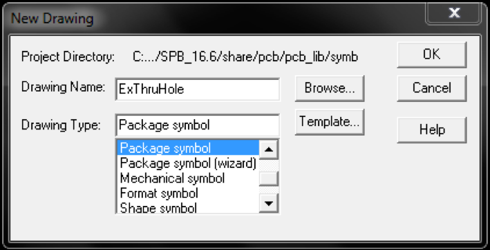
C:\Program Files\Cadence\SPB_17.4\share\pcb\pcb_lib\symbolsWhen creating a new footprint drawing, the New Drawing dialog box will show the default path (see Figure 1 below). If the path in the dialog box is different than the path above, use the dialog box path for the remainder of this tutorial.
|Figure 1: New Drawing dialog box
Also, note the exact name of the footprint. This will be needed later in order to reference it.
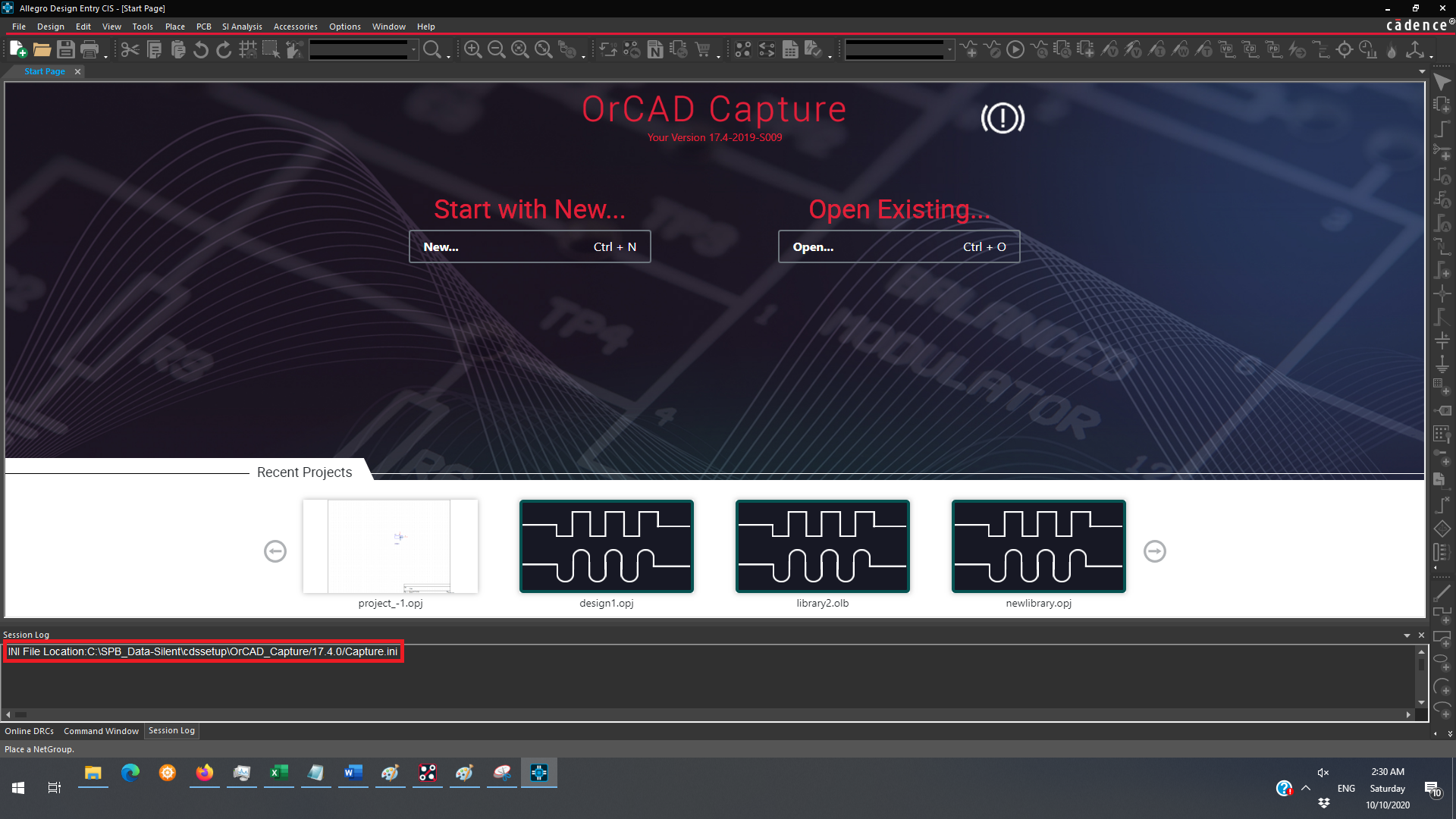
- Launch Design Entry CIS. Note the full path for the Capture.ini file shown on the Start Page (see Figure 2). Depending on how Cadence is installed on your computer, the full path should be similar to:
C:\Cadence\SPB_Data-Silent\cdssetup\OrCAD_Capture\17.4.0\Capture.ini
or, if you made a custom HOME variable: %HOME%\cdssetup\OrCAD_Capture\17.4.0\Capture.ini
Figure 2: Design Entry CIS Start Page |
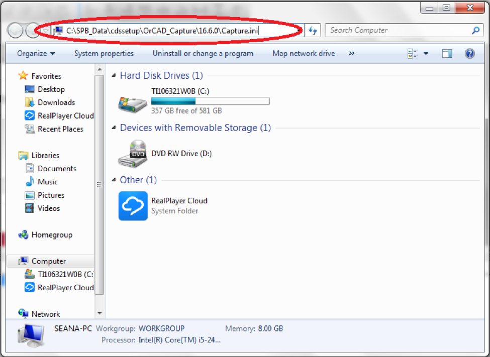
- Copy (Control-C) the full path of the Capture.ini file. Open the File Explorer in Windows, paste the full path into the path bar (see Figure 3), and press return.
Figure 3: Capture.ini file path in the File Explorer. |
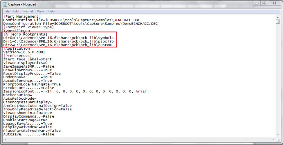
- The Capture.ini file will open in Notepad. Under the [Allegro Footprints] section, add the full library search path from step 1 above if it is not already listed (see Figure 4). Note that you must increment the number after Dir for each path added (e.g., Dir0, Dir1, Dir2). Do not delete any existing paths from the list. ** **
Figure 4: Capture.ini file with several library search paths added |
- You have successfully added a library search path to Design Entry CIS. If you are still not able to attach your custom footprints to schematic symbols, re-check the above steps and make sure your custom footprint name is correct.
Based on a tutorial written by Seana O’Reilly.


