Changing a Hole Diameter in Cadence PCB Editor
Why would you need to change the hole diameter?
The default diameter of holes in Cadence is 0.3 mm. This is too small for most components to fit through, as well as too small for proper through-plating of vias. According to the Peralta PCB Mill specifications, hole diameters should be at least 0.5 mm (19.7 mil). Therefore, the following settings are recommended:
- Drill diameter > 20 mil
- Pad diameter = drill diameter + (at least) 30 mil
- Soldermask diameter = pad diameter + 20 mil
Example: If the drill diameter = 31.5 mil, the pad diameter = 61.5 mil and the solder mask = 81.5 mil.
How do you change the hole diameter in PCB Editor?
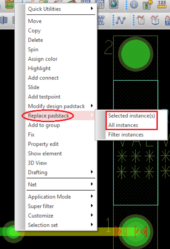
- In PCB Editor, open your design and right-click on a via or hole and choose “Replace padstack”. If you want to only change the selected via or hole, choose “Selected instance(s)”. If you want to change all vias or holes on your board, choose “All instances” (see Figure 1). The “Select a padstack” dialog box appears (see Figure 2).
Figure 1: Replace pad stack contextual menu |
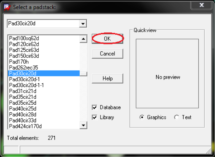
- In the “Select a padstack” dialog box, select Pad62cir32d (which has a 62 mil pad and a 32 mil hole) or another pad with a hole size of at least 20 mil and click OK (see Figure 2). While the hole size is reasonable for many components, the pad size is still too small.
Figure 2: Select a padstack dialog box |
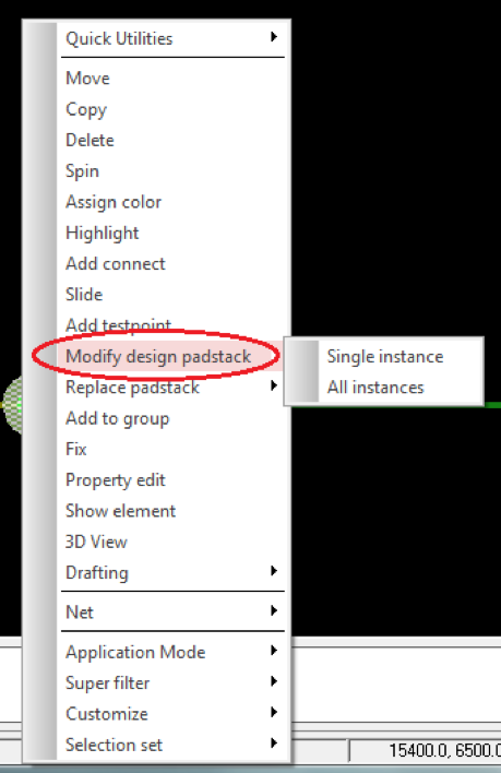
- Or you can modify the existing Padstack in your design. Right-click again on a via or hole and choose “Modify design padstack”. If you want to only change the selected via or hole, choose “Selected instance(s)”. If you want to change all vias or holes on your board, choose “All instances” (see Figure 3). The “Padstack Editor” dialog box appears (see Figure 4).
Figure 3: Modify design pad stack contextual menu |
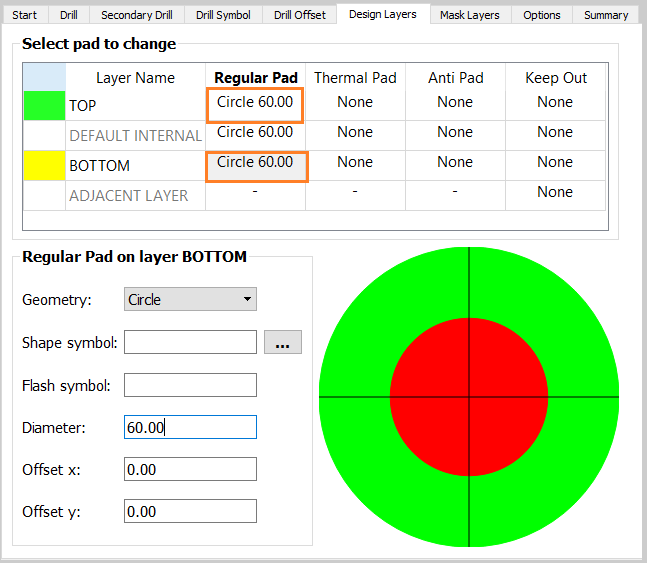
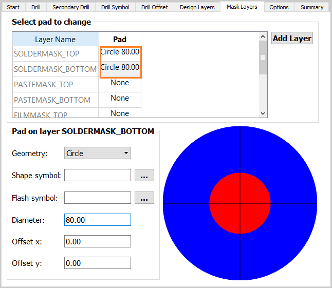
- In the “Padstack Editor” dialog box, increase the “Regular Pad” diameters to 60.0 or greater on the TOP and BOTTOM layers (see Figure 4), and change the Mask Layers diameters to 80.0 (see Figure 5).
Figure 4: Padstack Editor dialog box |
Figure 5: Padstack Editor dialog box - Mask Layers tab |
- In the “Padstack Designer” dialog box, choose File > Update to Design and Exit. You have successfully increased the pad size of the via or hole.
Based on a tutorial by Seana O’Reilly and updated by Qinchen Zha
