Adding Text to a Layout in Cadence PCB Editor
Introduction
Text is important on PCB layouts to identify the designers, project, version, components, etc. Typically, text can be placed on a silkscreen layer that sits on top of the copper. However, our manufacturing process in PRLTA 109 only supports text that is milled on the TOP COPPER or BOTTOM COPPER layers.
Note: It is required that all PCB designs have your name, course, and team number so that the Peralta Engineering Studios staff can distinguish your board from others.
How do you create millable text in Cadence PCB Editor?
-
Open your design in PCB Editor
-
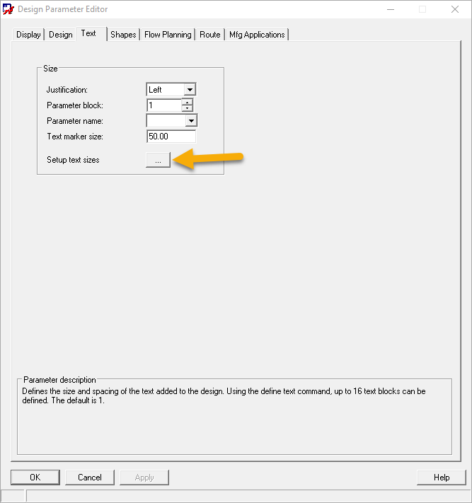
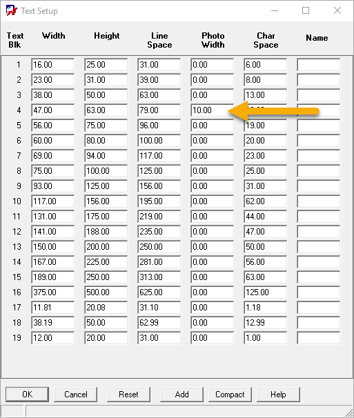
Choose Setup > Design Parameters… and click the Text tab. Click the … button next to Setup text sizes (see Figure 1). The Text Setup window will open (see Figure 2).
Figure 1: Design Parameter Editor Text tab |
Figure 2: Text Setup window |
-
In the Text Setup window, change the Photo Width for Text Blk 4 to 10.00 (see Figure 2). The 4th text value is big enough to read but not overly large. Click OK and OK to return to your design.
-
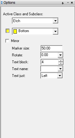
Click the abc+ button in the toolbar (see Figure 3) and click on the Options tab on the right hand of the screen (see Figure 4).
Figure 3: Add Text button |
Figure 4: Options tab configured for the 4th text block |
-
Configure the options to make sure the Top or Bottom layer is selected, and that the Text block is set to 4 (or whichever one that you changed in step 2) (see Figure 4).
-
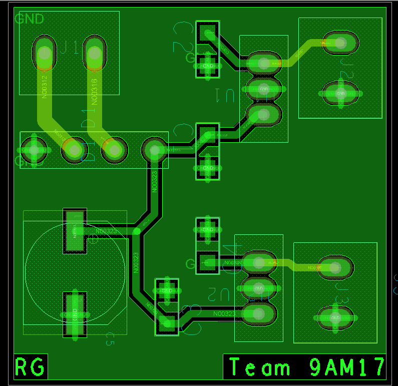
Click anywhere on the board and type the text that you wish to add (see example, Figure 5).
Figure 5: Example text on a layout |
Based on a tutorial by Robert Goby


